From the views of suppressing the switching stress and ensuring wide ZCS operation region, the value of 兝 is suitable between 兝=0.5 and 兝=0.8. Consequently the circuit is designed so that the value of 兝is set to 兝= 0.5 at Curie temperature and is set to 兝=0.8 at exceeding Curie temperature. As for the value ofp, p=0.2 is suitable as the value of suppressing the switching stress.
丂
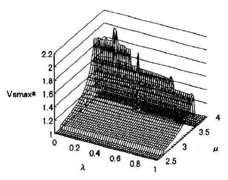
Fig. 8 Distribution of Vsmax*
(兛=0.05, 兝=0.5, p=0.2)
丂
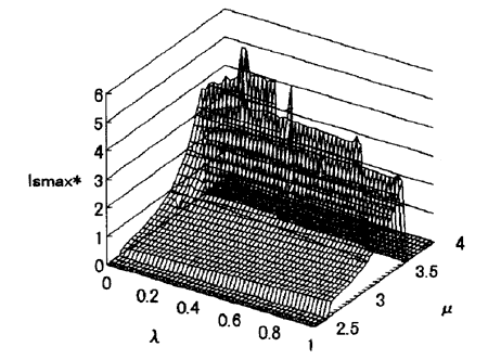
Fig.9 Distribution of Vsmax*
(兛=0.05, 兝=0.8, p=0.2)
丂
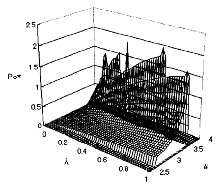
Fig. 10 Distribution of Ismax*
(兛=0.05, 兝=0.5, p=0.2)
丂
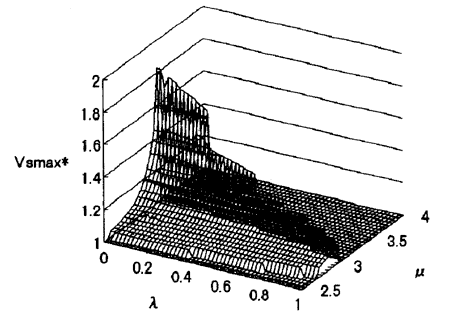
Fig. 11 Distribution of Ismax*
(兛=0.05, 兝=0.8, p=0.2)
丂
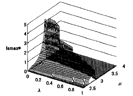
Fig. 12 Distribution of Po*
(兛=0.05, 兝=0.5, p=0.2)
丂
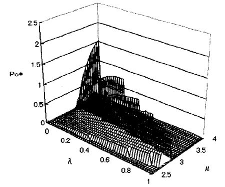
Fig. 13 Distribution of Po*
(兛=0.05, 兝=0.8, p=0.2)
丂
丂
4.3 Switching stress within ZCS operation region
Fig. 8 and Fig.9 show the distribution of the maximum voltage of switch of Vsmax* as switching stress within ZCS operation region at 兝=0.5 and 兝=0.8, respectively. In these figures, Vsmax* is suppressed to less than 1.2 in case the normalized frequency of 兪 is less than 兪=3.0.
丂
丂
丂
BACK丂丂丂CONTENTS丂丂丂NEXT
丂