The testing machine was stopped for each combination of the load x test time, and the surface profile of both test specimens after the test was measured by the surface roughness tester.
丂
2.2丂Test Results and Examination
2.2.1丂Reappearance of Partial Contacting Phenomenon
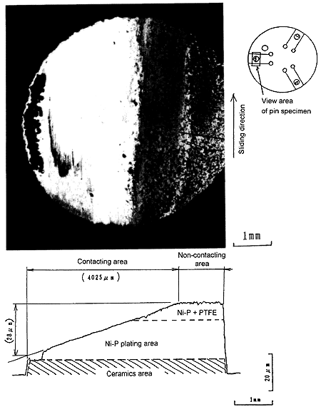
Fig. 3 shows an example of the result of the partial contacting wear test. This the worn surface of the Ni-P + PTFE plated pin specimen, which was subjected to the test of 4500N x 0.5 Hr after the test of 1500N x 0.5 Hr. The measured results of the surface roughness were compared with the observation results by the optical microscope
It is clarified that the partial contacting was generated in the pin specimen, and a part of the spray coated ceramics of the base material is exposed on the outer-most circumferential part where the partial contacting is severest. The film thickness of the Ni-P + PTFE plating can be measured from the difference between the exposed surface and the initial surface (the upper right of the surface profile of which plating is not yet brought into contact with the disk specimen, and the measurement of the inclination proved to be 28 兪m/4025 兪m, i.e., 35 兪m/5000 兪m, indicating the inclination approximately as indicated).
丂